Home / Research
Research
Perovskite solar cells now approach the efficiency of conventional silicon, but to reach industrial production several barriers must be overcome at once: material purity, interfacial chemistry, crystallization kinetics, device stability and scalable manufacturing. The group puts materials chemistry and device physics on the same bench, giving rise to five interlocking research directions.
Direction 01
Novel photoactive materials design
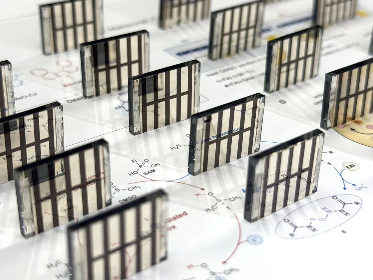
The molecular structure of interfacial and transport materials often sets the ceiling for device efficiency. Taking "chemical compatibility" as its central design principle, the group systematically develops functional molecules for perovskite photovoltaics: carbazole-based phosphonic acid self-assembled monolayers (SAMs) and their derivatives, conjugated hydrazide additives, symmetrical molecules with long-range-ordered π–π stacking, and hybrid molecular systems for interfacial passivation and charge extraction.
The question we care about is not simply whether a material conducts well, but what happens between it and the precursor, the solvent and the perovskite surface under real film-forming conditions. This perspective was shown in our 2026 Science paper to be the key to understanding a device performance bottleneck.

Direction 02
Perovskite photovoltaic technologies
Taking the inverted (p–i–n) architecture as the main line, we engineer both the buried interface and the top interface: through molecular hybridization, surface transformation and control of crystallization kinetics, we improve open-circuit voltage, fill factor and long-term stability at the same time.
On stability, our concern is not only whether a device lasts long, but where the degradation mechanisms come from. A 2023 Nature paper proposed homogenizing the vertical cation composition to suppress phase segregation; a 2024 Nature paper used buried-interface molecular hybridization to improve interfacial contact; and a 2025 Nature Materials paper revealed how PCBM dimer formation drives device degradation and offered a strategy to suppress it.

Direction 03
High-purity precursors & perovskite microcrystals
Device reproducibility begins with the raw materials. The group has developed a perovskite precursor synthesis route that uses water as the solvent, replacing conventional organic-solvent processes that are costly and environmentally burdensome, while markedly improving precursor purity and batch-to-batch consistency — published in Science in 2024.
Building on this, we continue to advance the precise synthesis and compositional control of perovskite microcrystals, studying crystal growth kinetics, defect chemistry and impurity control to provide a stable and reliable materials foundation for high-efficiency devices.

Direction 04
Lead halide perovskite recycling
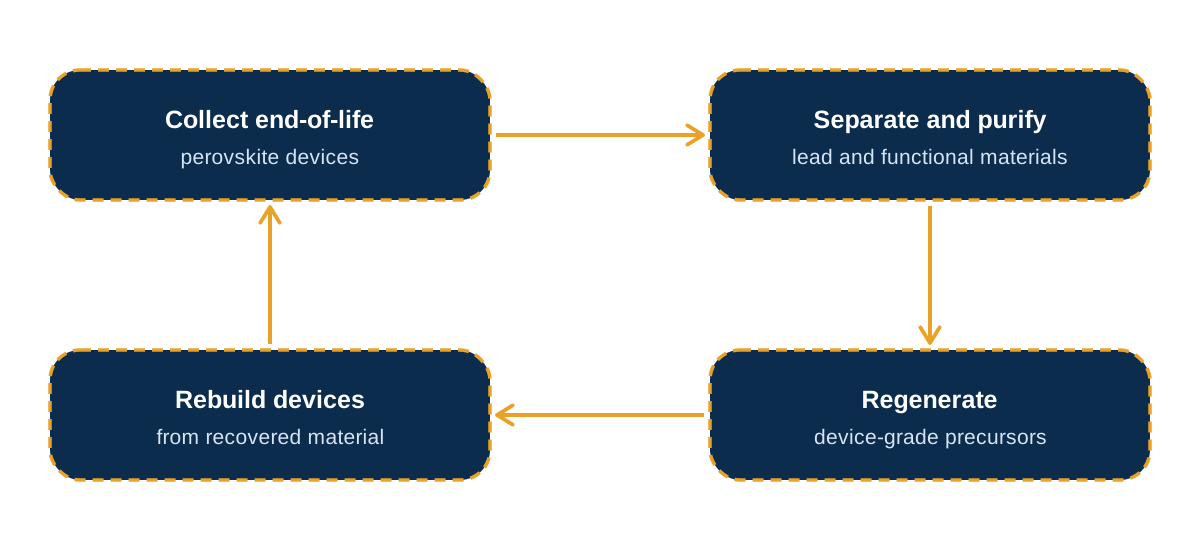
For perovskite photovoltaics to become a genuinely "green" energy technology, two questions must be answered: where does the lead go, and can the materials return to the production line? The group is systematically studying closed-loop recycling pathways for lead halide perovskites — separating, purifying and regenerating perovskite precursors and functional-layer materials from end-of-life devices, while exploring the valorization of solvents and additives.
Alongside this comes greener fabrication: reducing the use of toxic solvents, lowering energy consumption and improving material utilization, so that scalable manufacturing also holds up on environmental grounds.
Direction 05
AI-assisted photovoltaic research & development
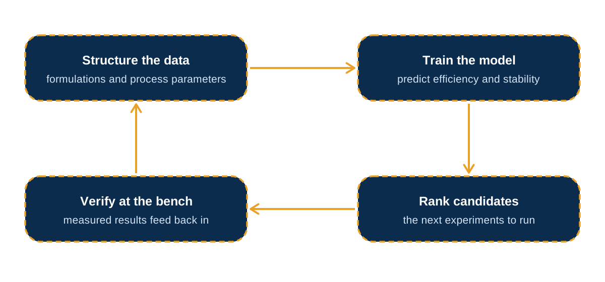
The compositional space and process window of perovskites are enormous — manual trial-and-error cannot exhaust them. The group explores a data-driven approach to R&D: structuring formulations, process parameters and device performance into datasets, and combining them with machine-learning models for high-throughput screening and process optimization, concentrating experimental resources on the most promising directions.
This direction is deeply coupled with experiment — the models produce actionable experimental suggestions, not conclusions on paper.
Platform
Drawing on the first-class shared research platform of the Function Hub at HKUST (Guangzhou) and the Wilson Tang Brilliant Energy Science and Technology Lab (BEST Lab), the group has a complete experimental loop from materials synthesis to device validation.
Gloveboxes, Schlenk lines and solvent purification systems support the controlled synthesis of precursors and functional molecules.
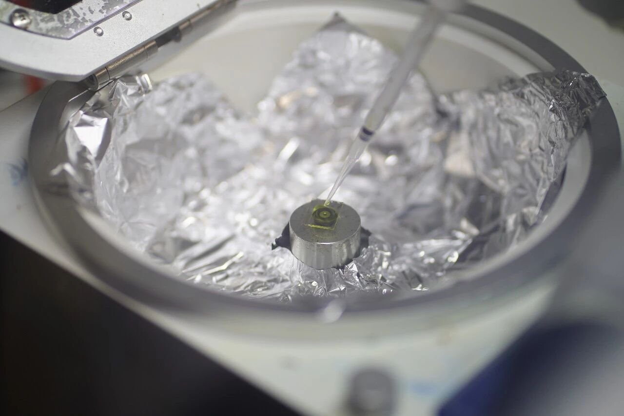
Spin-coating, blade-coating and slot-die coating, covering small-area devices through to module-scale validation.
J–V measurements, EQE, steady-state and time-resolved PL, transient absorption spectroscopy and other carrier-dynamics characterization.
MPPT tracking, damp-heat ageing at 85 °C / 85% RH, and light and thermal cycling reliability tests.
XRD, SEM/TEM, XPS, NMR and liquid chromatography, supporting analysis from crystal structure to chemical reaction mechanisms.
First-principles calculations, molecular dynamics and machine-learning modelling, forming a cross-validation loop with experiment.

Whether your strength is synthesis, devices, characterization or computation, the group welcomes you to join and collaborate.